Joining Rebellions in 2021, I was immediately tasked with a critical project: emulating the Atom chip. This was no small feat, as the Atom boasted a staggering 1.55 billion gates, making its mapping to FPGAs a significant challenge.
The lengthy Place and Route (P&R) process, in particular, proved to be a major hurdle, requiring many late nights and early mornings. However, after months of dedicated effort, we successfully built the system, and its subsequent use in the emulation environment proved incredibly valuable, filling me with a sense of accomplishment.
System Architecture
The overall system was constructed using a Synopsys HAPS-100 prototyping system alongside 9 Xilinx U250 boards.
To handle the sheer scale of 1.55 billion gates, we adopted a strategy of partitioning the entire system by function:
- Neural Engine Offloading: The Neural Engine, responsible for the Atom chip’s most computationally intensive and repetitive operations, was offloaded to the U250 boards.
- High-Speed I/O (HSIO): Interfaces were used to facilitate data transfer between the HAPS-100 and the U250s. We employed Xilinx Aurora IP for the physical layer and developed a custom protocol on top of it to efficiently transmit data, clocks, and reset signals.
- Shared Memory: Due to the Atom chip’s large on-chip SRAM requirements, we offloaded the shared memory to a dedicated U250 board.
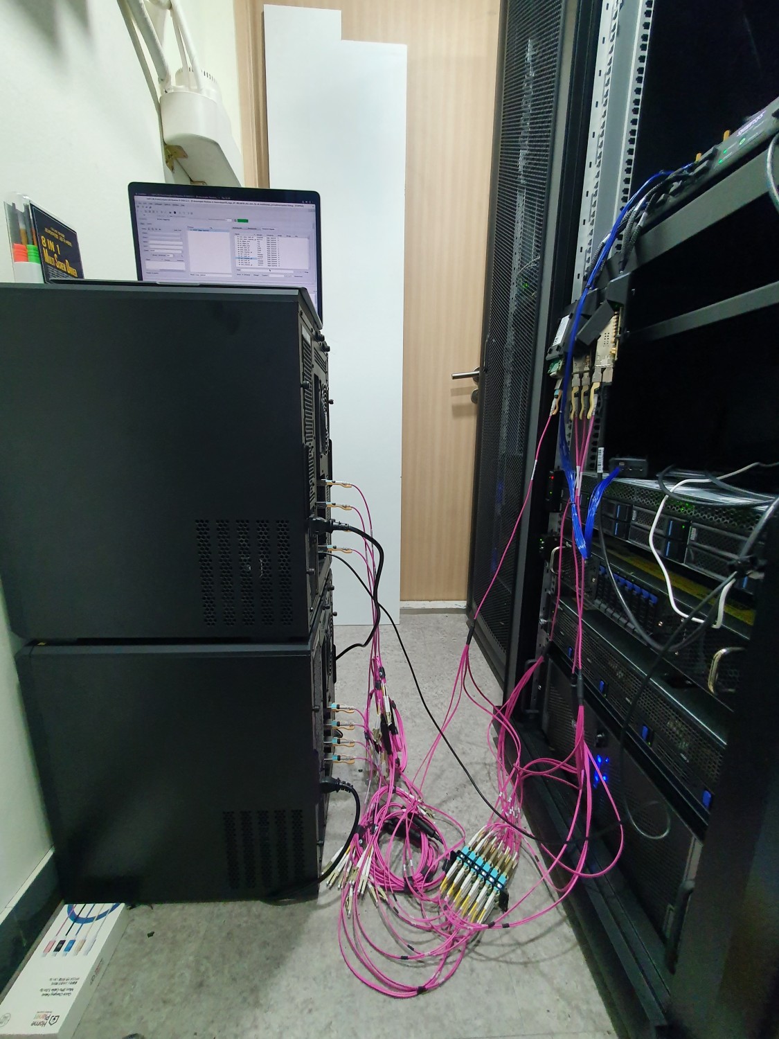 Figure 1: The complete Atom chip emulation system, showcasing the HAPS-100 and 9 Xilinx U250 boards linked through high-speed QSFP optical cables.
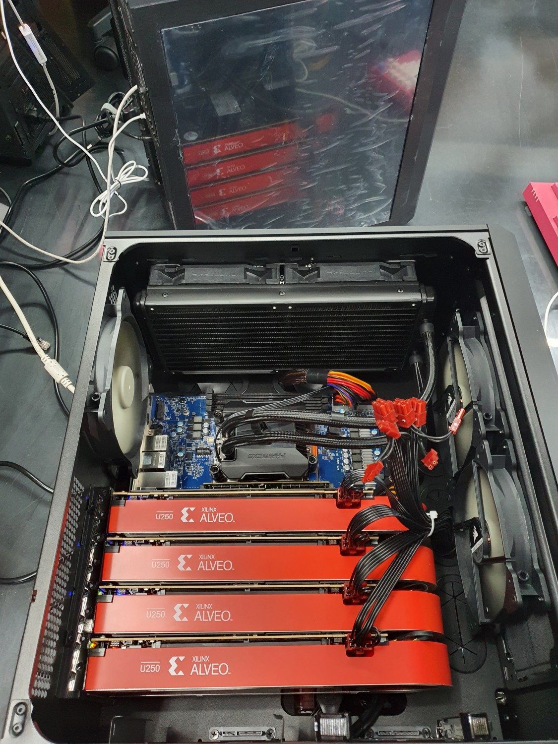 Figure 2: U250 Installation: While only requiring a power supply, the U250s were installed in workstations for enhanced stability.
Overcoming Routing Bottlenecks in the HAPS-100
The implementation of data buses and cache logic within the HAPS-100 resulted in severe routing congestion, leading to repeated implementation failures. The HAPS-100 houses 4 VU19P FPGAs, interconnected via LVDS links. Each VU19P is itself a chiplet structure comprised of 4 dies (SLRs), limiting inter-die connectivity.
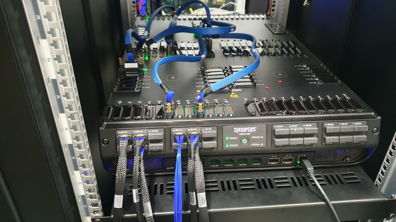 Figure 3: HAPS-100 HT3 Interconnect Wire Structure.
To address these routing congestion challenges, we implemented the following technical solutions:
- AXI Bus Partitioning: The AXI bus was physically divided into read (R) and write (W) operations. Furthermore, a hierarchy was built within each block to ensure logic mapping remained within a single die where possible.
- Addressing SSI Resource Limitations: To overcome the scarcity of Stacked Silicon Interconnect (SSI) resources for inter-die communication, we introduced SerDes logic between the dies to drastically increase the available bandwidth per line.
- Data Bus LVDS Bundle Mapping Control: The HAPS automatic partitioning process, while distributing LVDS I/Os evenly, resulted in the concentration of the data bus within specific LVDS bundles, causing congestion. We manually adjusted this to distribute the data bus across multiple LVDS bundles evenly.
Conclusion
The FPGA mapping process for the Atom chip emulation presented unexpected complexity and significant challenges. However, through a combination of innovative technical solutions and persistent problem-solving efforts, we were ultimately successful in building the system, making a substantial contribution to Rebellions’ chip development process.
In particular, the experience gained in resolving routing congestion within resource constraints and optimizing system performance will be invaluable for designing and implementing more complex systems in the future.
➡️ Continue reading: Part 2 - Mastering Routing Congestion and Partitioning